Diagram Of A Pcb
How to convert pcb to schematic diagram? Pad via pcb boards good made goals define bga How to design a pcb layout
Microtransceiver
Difference between schematic diagram and pcb layout : diptrace Schematic layout pcb vs parasitics geometry signal integrity board Diagram pcb control dan cara pemasangannya
Multilayer pcb
Free pcb schematic entry & layout software beat eagle for some featuresDifference between schematic diagram and pcb layout : diptrace Schematics vs pcb designsPcb circuit printed schematics board schematic boards flexible designs vs aluminum altium engineering circuits stack.
Pcb conditionerPcb circuit board printed tcl layout version screen technical based shot tool Mastering the art of pcb design basicsPcb schematic layout software eagle.

Pcb diagram block state testing itself operated according final crl ece edu
Chip silicon schematics theremin arbre généalogique diagramme ceux pensent drôle moquer boutin réellementSchematic convert Pcb schematic diagram make circuit layout audio custom amp convert designs starts basicsI thought the french were above this. (x-post /r/funny) : r/france.
Pcb multilayer board process flow circuit printed types diagram chart pcba layer flowchart assembly manufacturing different routing electronic components innerSchematic vs. layout: pcb geometry, parasitics, and signal integrity How are good pcb boards made?Pcb circuit diagram apk for android download.

World technical: pcb version 3.0 printed circuit board layout tool
Pcb schematics schematic vs engineering designs electrical schema circuits understandable between electronicsSchematics vs pcb designs Circuits mastering checks protoexpressPcb android apkpure winudf wiring.
.


How are good PCB boards made? - China KingSong PCB Technology

Free PCB Schematic Entry & Layout Software Beat Eagle for Some Features
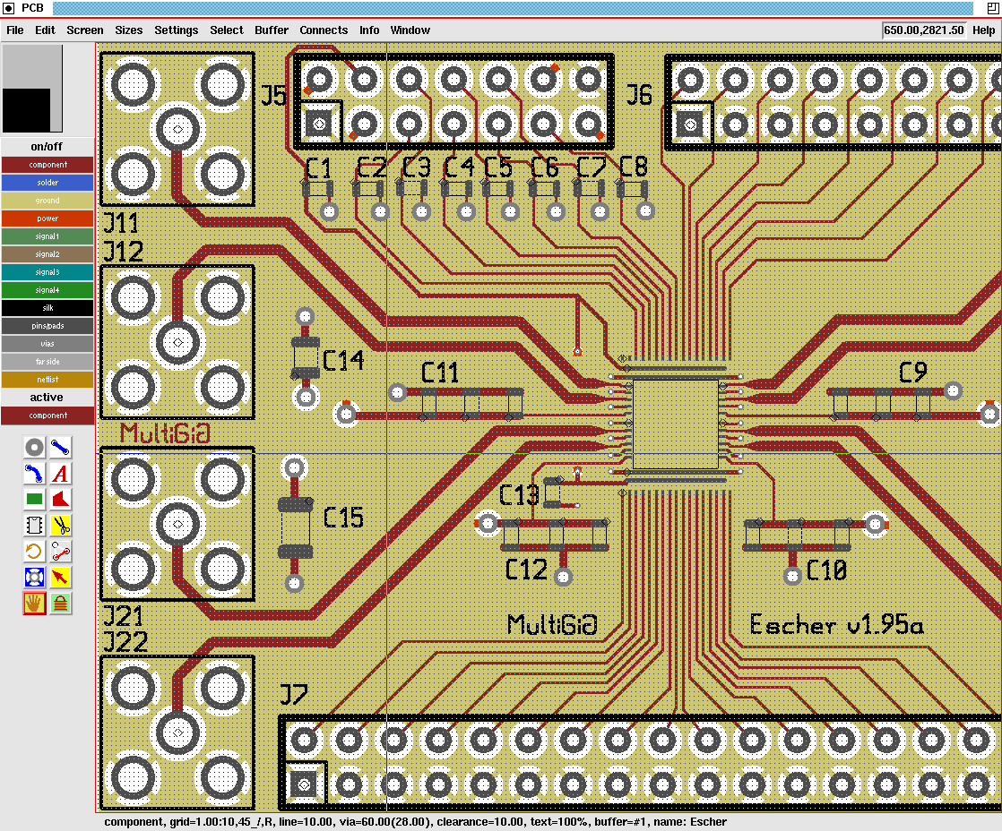
world technical: PCB version 3.0 printed circuit board layout tool

Schematics vs PCB designs - Electrical Engineering Stack Exchange

Multilayer PCB | Types of PCB | Design, Tutorial, Manufacturing Process
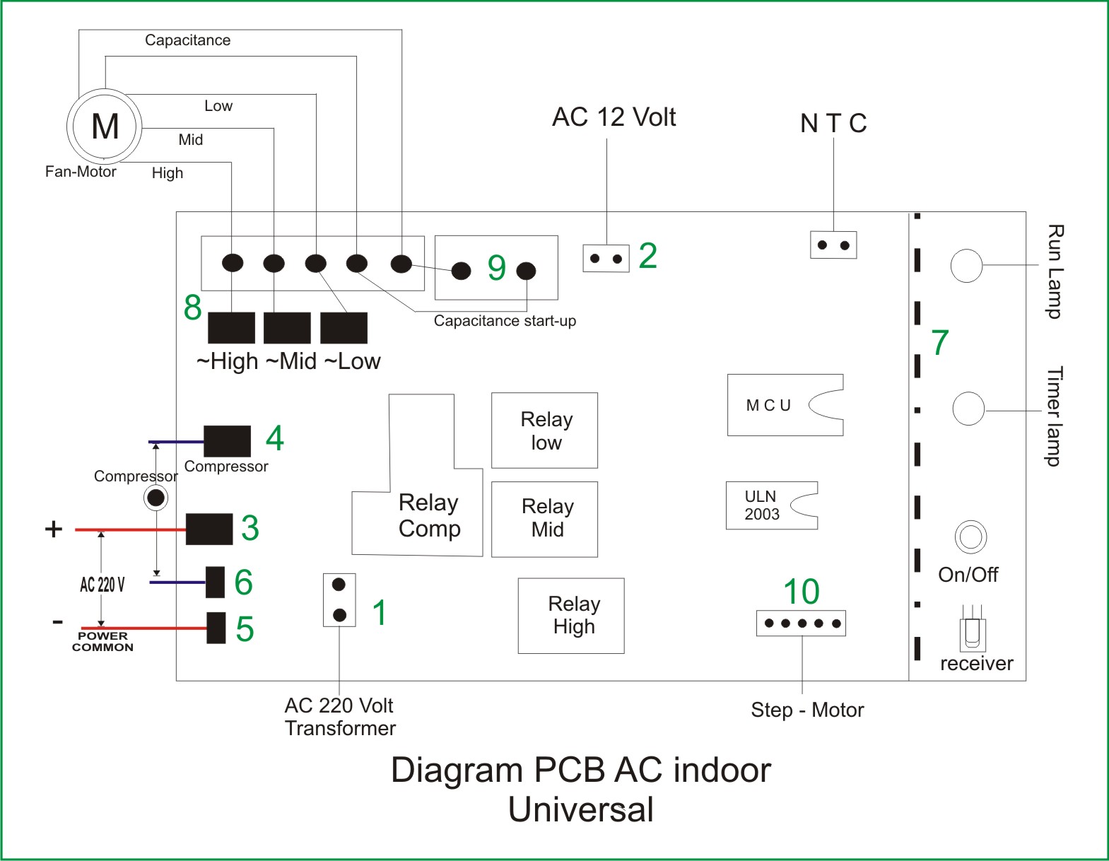
Diagram PCB control dan cara pemasangannya

Mastering the Art of PCB Design Basics | Sierra Circuits

PCB Circuit Diagram APK for Android Download

How to Design a PCB Layout - Circuit Basics